

Work on real-world challenges from the
semiconductor and electronics ecosystem.
Build practical
solutions, receive guidance from industry experts and
compete for the opportunity to showcase your
work at SEMICON India 2026.
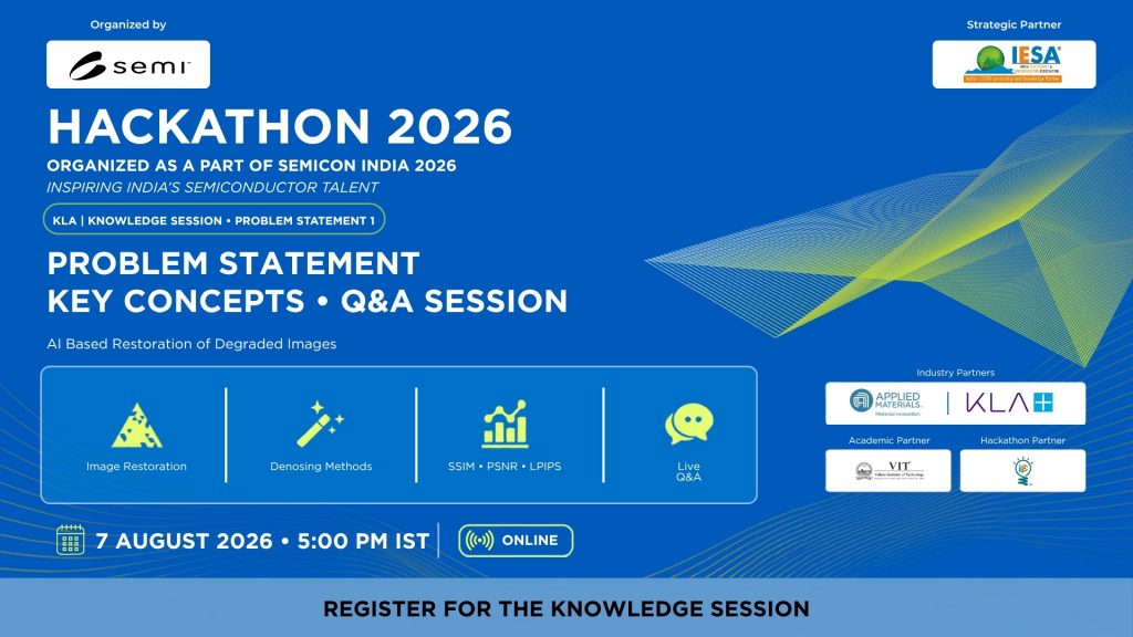
Build breakthrough solutions for AI defect classification for semiconductor wafer/die images. Grand Finale at IESA Vision Summit 2026 (Bengaluru) — pitch to IESA leadership + top industry experts.
Build Solutions for India’s Semiconductor Future
The Hackathon is India’s, national student hackathon embedded within SEMICON India, the country’s flagship semiconductor and ESDM trade show. Designed to connect India’s engineering talent with the real technical challenges facing the semiconductor industry, this hackathon asks teams to move beyond ideas and build solutions that matter: in chip design, AI-enabled manufacturing, yield optimisation, and advanced verification.
This hackathon is structured to produce outcomes, not just participation. Teams move from a real industry-defined problem statement to a working prototype, evaluated on technical depth, innovation, feasibility, and deployment potential, supported by domain mentorship from KLA and Applied Materials engineers, and a transparent multi-round evaluation framework. Top finalists pitch live at SEMICON India 2026 in front of global semiconductor leaders.
India's Union Cabinet has approved Semicon 2.0 with Talent Development as its Sixth Pillar, a national mandate to build 1 lakh+ design engineers, equip 500+ institutions with EDA tools, and establish new semiconductor manufacturing training infrastructure across the country. This hackathon is a direct contribution to that mission.
Over the next 5 years, India will produce a generation of chip design, VLSI, and EDA-proficient engineers capable of supporting India’s fabless and design-led semiconductor growth.
New training facilities will be set up for semiconductor manufacturing skills in fabrication, OSAT packaging, and equipment operation in partnership with industry and state governments.
The Hackathon 2026
is a direct industry-action aligned
with Semicon 2.0 where real problems
from KLA and Applied Materials
become the training ground for India's
next generation of semiconductor engineers.
India's semiconductor ambition is real, driven by the India Semiconductor Mission, policy momentum from MeitY, and billions in committed fab and ATMP investment. But ambition without talent is strategy on paper. India needs engineers who can work on chip design, yield optimisation, AI-in-EDA, and advanced verification, not in theory, but in practice.
The Hackathon 2026 creates a national platform where high-potential engineering talent builds industry-ready solutions to real semiconductor challenges, guided by engineers from KLA and Applied Materials, and evaluated by senior industry experts. Finalists walk off the SEMICON India stage with visibility, credibility, and career opportunities that no placement drive can replicate.

Builds talent in AI-enabled chip design and semiconductor manufacturing, two of the fastest-growing skill areas in India's ESDM roadmap.

Identify promising students with capabilities in chip design, verification, manufacturing analytics, embedded systems and AI-enabled engineering.

Give students access to industry mentors, technical evaluators and ecosystem leaders whileav helping companies engage emerging talent.

Finalists pitch live at SEMICON India 2026 in front of exhibitors and global semiconductor leadership unique advantage no campus event offers.
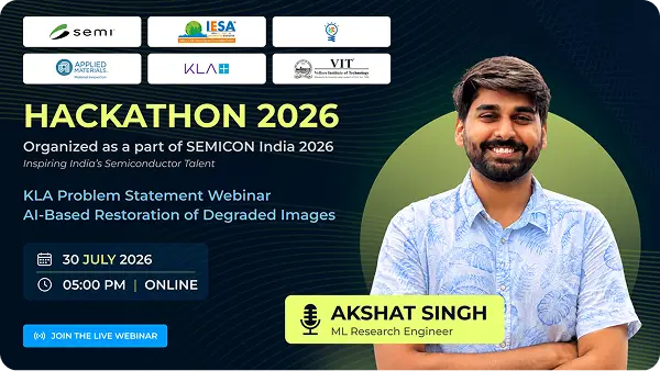
In semiconductor manufacturing, microscopic inspection images are used to measure and verify chip quality at every stage of production. These images must be extremely sharp and clean because a single pixel of noise or a small loss of detail can hide a defect that causes a chip to fail.
In practice, inspection images are often degraded by two types of signal loss:
Currently, engineers work with these degraded images and make do with the noise and lost detail. AI-powered restoration can recover information that appears lost removing noise while sharpening detail back to the original resolution.
You will receive a training dataset of paired images: for each sample, you get a degraded image (noisy + low resolution) and the corresponding ground truth image (clean + full resolution). Your job is to train an AI model that learns to reverse the degradation taking a bad image as input and producing a restored image that matches the ground truth as closely as possible.
The degradation types your model must handle:
Degradation Type | What It Looks Like | What Your Model Must Fix |
Speckle Noise | Random pixel-level noise, image looks grainy. Some pixel values are pushed beyond the true range of the image. | Remove the grain while preserving the real image details underneath. Do not blur the image to remove noise, that destroys useful information. |
Gaussian Noise | Image appears soft and hazy edges and fine structures lose sharpness. | Restore edge sharpness and contrast without introducing artificial patterns or ringing. |
Spatial Resolution Reduction (Super-Resolution) | Image has been downsampled: 512×512 → 256×256, or 256×256 → 128×128. Fine details are lost. | Upscale the image back to the original resolution (512×512 or 256×256) while reconstructing the fine details that were lost during downsampling. |
Training Data — What You Get
KLA will provide a paired training dataset. For each sample, you receive:
What You Get | Resolution | Description |
Ground Truth Image (clean, full resolution) | 512×512 pixels or 256×256 pixels | The ‘correct answer’ — the image as it should look. High resolution, high signal-to-noise ratio. This is what your model’s output should match. |
Degraded Image (noisy, low resolution) | 256×256 pixels or 128×128 pixels | The input to your model — noisy and downsampled. Your model takes this as input and must produce an output that matches the ground truth. |
Important data notes:
Test Data — What Comes Later
After the training phase, KLA will release a test dataset. The test set contains:
All submissions are made through the i4C hackathon portal. You must submit a PPT/PDF using the provided Idea Submission Template AND a GitHub repository link. Here is exactly what each must contain:
Component 1 — PPT/PDF Submission (Using Idea Submission Template)
Use the provided Hackathon Idea Submission Template. Fill in each slide as follows:
Template Slide | What to Fill In |
Slide 1: Team Details | Team name, member names, roles, college name, contact details. |
Slide 2: Problem Statement Addressed | Select ‘AI-Based Restoration of Degraded Images.’ Describe in your own words why this problem matters in semiconductor manufacturing. |
Slide 3: Idea Description | Your key concept and approach – what type of AI model did you choose? Why? How does it address all 3 degradation types (speckle, Gaussian, super-resolution)? |
Slide 4: Proposed Solution | Detailed solution – model architecture, training strategy, loss function design, data augmentation approach. Include a system/pipeline diagram. |
Slide 5: Innovation & Uniqueness | What makes your approach different? Did you design a novel loss function? A unique data augmentation strategy? A faster inference pipeline? |
Slide 6: Results | SSIM, pSNR, LPIPS scores on your test split. Before/after image comparisons (degraded input → your restored output → ground truth). Confusion-free visual evidence that your model works. |
Slide 7: Technology & Feasibility | Tech stack used (PyTorch/TensorFlow/other), hardware used for training (GPU type, cloud platform), training time, model size, inference time per image. |
Slide 8: GitHub & Video Link | GitHub repository link (mandatory). Video link showing your model running (optional but recommended). |
Slide 9: References | Research papers, datasets, tools referenced. |
FILE FORMAT: Save as PDF before uploading. File naming convention: TeamName_KLA_PS01 (e.g., VisionForge_KLA_PS01.pdf). Maximum 8-9 slides. Remove the instruction slide.
Component 2 — GitHub Repository (Mandatory)
Your GitHub repository must be public and must contain:
# | Repository Content | Details |
1 | README.md | Complete setup instructions. A reviewer must be able to clone your repo and run inference from the README without contacting you. |
2 | Evaluation Script (standalone .py) | A Python script (NOT a Jupyter notebook) that accepts: (a) path to test images directory, (b) path to output directory. It loads your trained model, runs inference on all input images, and writes restored outputs to the specified directory. Must run without manual edits. |
3 | Training Script | Python script or Jupyter notebook that reproduces your training process from scratch. |
4 | Trained Model Weights | Your final trained model file (in a format your evaluation script can load — .pt, .onnx, .h5, etc.). Must be downloadable (use Git LFS or link to Google Drive/HuggingFace if file is large). |
5 | Restored Test Outputs | A folder containing your model’s output on the test set — the actual restored images your model produced. |
6 | requirements.txt | Complete pip freeze output from your training environment. Required for reproducibility. |
CRITICAL: The evaluation script is the most important file in your repository. It will be used AS-IS by KLA’s benchmarking team to measure your model’s quality scores and inference time on the H100 GPU. If your script does not run without manual edits, your submission cannot be benchmarked and unscored submissions cannot win. Test your script on a fresh machine before submitting.
A modern wafer inspection tool must return to exactly the same site on a die – thousands of times per day, across hundreds of dies on every wafer. The first visit is straightforward: the tool finds the target site and records its location. Every subsequent visit must land at the identical spot with nanometre accuracy so that measurements are comparable across time and across different tools.
In practice, this does not happen perfectly. Motion stages accumulate tiny errors between visits drift from thermal expansion, vibration from the fab environment, and mechanical slack. These errors compound over time. By the time the tool revisits a site on a different die (or on the same die hours later), it may land several pixels away from the intended location.
Because all dies on a wafer carry the same repeating circuit layout, the tool cannot simply look at the landed image and know it is wrong the structure at the wrong location looks almost identical to the correct one. This is the core difficulty: finding a specific site inside a sea of visually similar repeating patterns.
Applied Materials calls this challenge Navigation-Error Recovery. It is solved today with classical template-matching algorithms, but these break down in highly periodic layouts (DRAM memory arrays, FinFET gate structures) where hundreds of nearly identical features are visible in the same frame. AI and advanced computer vision approaches offer a path to more robust, higher-accuracy recovery.
What your algorithm must produce:
Challenge | Why It Is Difficult |
High periodicity of die layouts | DRAM word-line/bit-line grids and FinFET fin arrays repeat with sub-pixel variation. Template matching returns false positives across the entire array. |
10x scale difference | The reference pattern is 100x magnification; the search image is 10x. The reference occupies approximately 100 x 100 pixels in the search image — about 1% of its area. |
Sensor noise differences | The reference and search images are separate physical captures — each has its own independent sensor noise. The reference is sharper; the search image is noisier (lower magnification means more noise). |
No proprietary dataset provided | Due to IP constraints, Applied Materials cannot share real wafer images. You must generate your own synthetic but realistic training and test data. |
No Dataset Is Provided — You Must Generate Synthetic Data
What Your Synthetic Dataset Must Look Like
Each training sample is an image pair: a Reference Image and a Search Image. You choose either DRAM-style or FinFET-style die architecture — both are judged equally.
Architecture Style | Reference Image Structure | Search Image Structure |
DRAM-style | Periodic horizontal word-lines and vertical bit-lines crossing at right angles, with a small contact/via dot at every intersection. High-contrast, fine pitch, extremely regular. | A larger tiled version of the same DRAM grid, downsampled to 1000 x 1000 pixels to represent the 10x lower magnification. The reference pattern appears shrunk ~10x somewhere inside. |
FinFET-style | Dense parallel vertical fin lines, crossed by one or two horizontal gate bars at the intersection region. High-contrast vertical structure with distinctive gate crossings. | Same approach — a larger tiled FinFET layout, downsampled to 1000 x 1000. The reference appears as a small ~100 x 100 pixel inset somewhere inside the search image. |
Mandatory Requirements for Your Dataset Generator:
Citation Requirement:
Every augmentation choice, noise model, and structural parameter you select must be justified with at least 2-3 credible public references — academic papers, textbooks, or patents on semiconductor device structure or SEM imaging. These citations must appear in your final presentation. Unjustified augmentation choices will not receive full marks on the 30% augmentation score.
STARTER SUPPORT: Applied Materials will provide a starter Python prompt (PIL/numpy) that generates one basic image pair showing the correct 1000×1000 pixel structure, 10x zoom relationship, and independent noise. This is a starting scaffold — not a complete dataset generator. Teams are expected to significantly extend it to add realistic variation, augmentation, and class diversity. A GitHub repository with additional code samples will be shared during the hackathon as per the event schedule
Test Data — What Applied Materials Will Use
Applied Materials will provide a separate set of synthetic image pairs as the official test set for Phase 2. This test set will:
Component 1 — PPT/PDF Submission (Using i4C Idea Submission Template)
Use the provided Hackathon Idea Submission Template. Fill in each slide as follows:
Template Slide | What to Fill In |
Slide 1: Team Details | Team name, member names, roles, college name, contact details. |
Slide 2: Problem Statement Addressed | Select ‘Drift-Sense: Navigation-Error Recovery.’ Describe in your own words why navigation-error recovery matters in semiconductor wafer inspection — use the Background section above as context. |
Slide 3: Idea Description | Your key concept and approach — did you choose DRAM-style or FinFET-style architecture? What localization algorithm did you select (classical ML or deep learning)? Why is your approach better than simple template matching for periodic layouts? |
Slide 4: Proposed Solution | Detailed solution — dataset generator design (architecture, noise models, augmentation), localization algorithm (architecture or method, key design decisions), pipeline diagram showing input pair to output (x, y). Include citations for every augmentation choice. |
Slide 5: Innovation & Uniqueness | What makes your approach different? Is your dataset generator more realistic than the baseline? Does your localization handle periodic ambiguity better? Did you find a novel approach to the 10x scale difference problem? |
Slide 6: Results | Accuracy rate on your own 30+ test cases: percentage of predictions within tolerance of true location. Computation time per image pair (1000 x 1000 pixels). One visual example of a SUCCESS case and one HONEST FAILURE case — where your algorithm went wrong and why. Visual: reference image, search image, your predicted location, true location. |
Slide 7: Technology & Feasibility | Tech stack (Python libraries used), hardware used for development (CPU/GPU, cloud platform), dataset generation time, localization inference time per pair, model size if DL method used. |
Slide 8: GitHub & Video Link | GitHub repository link (mandatory). Video link showing your algorithm running on a sample image pair (optional but recommended). |
Slide 9: References | All citations used to justify augmentation/noise choices. Research papers, patents, or textbooks on SEM imaging, semiconductor structure, or computer vision methods used. |
Component 2 — GitHub Repository (Mandatory)
Your GitHub repository must be public and must contain:
# | Repository Content | Details |
1 | README.md | Complete setup instructions. A reviewer must be able to clone your repo, generate a sample image pair, and run the localization algorithm from the README without contacting you. |
2 | Dataset Generator Script (standalone .py) | A documented Python script that generates synthetic image pairs (Reference + Search). Must accept parameters: architecture style (DRAM/FinFET), number of pairs to generate, output directory. Must record the true center coordinates of the reference pattern in each generated pair as ground truth. |
3 | Localization Inference Script (standalone .py) | A Python script that accepts: (a) path to reference image, (b) path to search image. Outputs the predicted center (x, y) of the reference pattern within the search image. Must run without manual edits. This is the script Applied Materials will run on test data. |
4 | DL Model Weights (if applicable) | If you use a deep learning approach, include model weights in a downloadable format (.pt, .h5, .onnx). Must be loaded automatically by your inference script. |
5 | Training Script or Notebook (if applicable) | If you train a model, include the training script or Jupyter notebook that reproduces your training process. |
6 | requirements.txt | Complete pip freeze output from your development environment. Required for reproducibility. |
7 | Citation Documents / Supporting References | PDF or markdown file listing all references used to justify augmentation and noise choices. Must correspond to the citations in your PPT presentation. |
CRITICAL — INFERENCE SCRIPT: The localization inference script is the most important file in your repository. Applied Materials will run it directly on their test image pairs to compute your Phase 2 score. It must run without manual edits, must accept a reference image path and search image path as inputs, and must output a single (x, y) coordinate. Test it on a fresh machine before submitting. An unrunnable script cannot be scored.
Team registration and initial solution submission open on the hackathon platform.
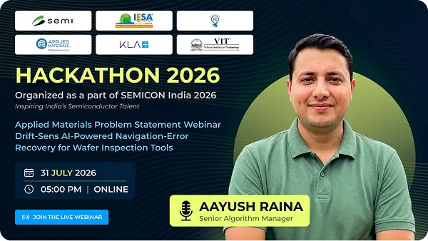
Detailed explanation of the problem statement, industry context, key challenges and expected solution outcomes.
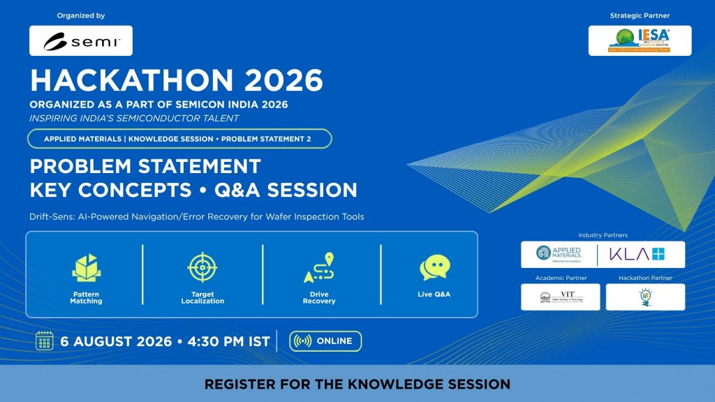
Domain-focused session covering relevant semiconductor technologies, technical requirements and possible solution approaches.
Expert guidance on developing an innovative, technically sound, feasible and scalable solution.
Q&A session for submission requirements, deliverables, submission format or technical queries.
Last date for teams to register for the hackathon.
Last date for registered teams to submit their initial solution proposals and supporting documents.
Subject-matter experts begin evaluating submissions based on innovation, technical approach, feasibility, impact and scalability.
The Top 30 semifinalists are announced. Round 2 tasks, deliverables and presentation guidelines are shared.
The Top 30 teams begin developing their enhanced solutions, prototypes, presentations and technical documentation.
Last date for the Top 30 teams to submit their Round 2 solutions and required deliverables.
Expert jury evaluates the Round 2 submissions, prototypes and team presentations.
The Top 10 finalist teams are officially announced. Grand Finale guidelines and mentoring schedules are shared.
Dedicated mentoring sessions for the Top 10 teams with technical, domain and industry experts.
Teams report to the Grand Finale venue for onboarding and event formalities.
The Top 10 teams present and demonstrate their solutions before an expert jury comprising semiconductor industry leaders.
Announcement and recognition of the winning teams of the SEMICON India Hackathon 2026.
Celebrate brilliance and innovation with exceptional prizes and prestigious recognition!
Total Prize Pool ₹5,00,000
TRACK 1 — KLA
TRACK 2 — APPLIED MATERIALS
Finalists get the opportunity to attend the summit and pitch on a high-visibility stage in front of IESA leadership and senior industry experts.
Exclusive hardware / development kits, tool credits, and goodies from sponsoring partners (subject to sponsor availability).
Certificates, digital badges, and feature highlights across IESA + i4C channels for top teams.
Direct networking with industry leaders, semiconductor & embedded experts, startups, and ecosystem partners at the summit.
Top teams get visibility for internships, hiring opportunities, and project collaborations with participating companies and partners.
Director
Design Enablement | AI | Digital Transformation - NXP Semiconductors
Mallikarjuna Bande is a semiconductor leader with 30+ years’ experience driving AI-enabled VLSI innovation.
Director
GlobalFoundries
Jay Shah, with extensive experience in semiconductor engineering focuses on semiconductor device design and characterization
Design Engineer at NXP Semiconductors
Reshma has 8 years experience, Masters from BITS Pilani, works at NXP designing 16nm libraries.
Principal CFM Defect Engineer
GlobalFoundries
She specializes in defect analysis, fault monitoring, and semiconductor yield improvement
Member of Technical Staff
GlobalFoundries
Safeer Afaque specializes in semiconductor automation, analytics, and AI-driven yield engineering.
Sr Business Automation Manager
CTO | Digital Transformation NXP Semiconductors
Amit Dad is a Business leader with 22 + years of experience in Automation
DFT Lead
Qualification | Design Enablement NXP Semiconductors
Avinash Kumar is a DFT engineer with 5 years of experience in DFT qualification, and enablement.
Defects Engineer
GlobalFoundries
He specializes in identifying yield-killing defects and root cause analysis in semiconductor manufacturing.
Head – Research & Innovation
Neilsoft | Secretary, i4C
A technology leader with 22+ years of expertise in software development, specializing in embedded systems and web applications.
Founder & CEO
10cTechClub
Startup entrepreneur and educator with 25+ years experience, founder of 10xTechClub delivering experiential learning.
Lead Subject Matter Expert
L&T EduTech
A passionate educator with 30+ years’ experience in engineering education, specializing in curriculum design, pedagogy, evaluation, and technologies.
Head - Embedded Systems
Aeron Systems Pvt. Ltd.
Bharat Kokate, Head of Embedded Systems and scrum Master, brings 17+ years’ expertise, mentoring innovation through hackathons.
Transform Tomorrow: Silicon to Systems
SEMICON India 2026 will bring together the semiconductor and electronics ecosystem to advance collaboration, innovation, manufacturing, skills and global partnerships. The event is scheduled for 17-19 September 2026 at Yashobhoomi (IICC), New Delhi, under the theme 'Transform Tomorrow'.
Exhibitors
Speakers
Sq ft Exhibition Space
State Pavilions
Eligibility
What You Need to Submit
Get all the details about the hackathon, including problem statements, timelines, prize information & FAQ.
Click below to download reference idea submission template.
Click below to know how to register for the hackathon.

SEMI is the global industry association that brings together the electronics design and manufacturing supply chain. In India, SEMI drives initiatives to strengthen India's semiconductor ecosystem, support policy development, and build a future-ready talent pipeline aligned with the India Semiconductor Mission. SEMICON India, organised by SEMI, is Asia's premier semiconductor and electronics event.

India Electronics and Semiconductor Association (IESA) is India's leading industry body for ESDM, semiconductors, and intelligent electronics, connecting industry, startups, academia, and policymakers to strengthen India's innovation and manufacturing ecosystem. IESA's Hackathon chapter builds directly on their commitment to talent development and industry-academia collaboration.
KLA is a global leader in process control and yield management solutions for semiconductor and related nanoelectronics industries. By sponsoring Problem Statement 1 — KLA brings one of the most critical real-world challenges in semiconductor manufacturing directly to Indian engineering talent, while building early access to a future-ready workforce.

Applied Materials is the world leader in materials engineering solutions used to produce virtually every new chip and advanced display in the world. By sponsoring Problem Statement — Applied Materials engages with India's top engineering talent on the challenge of making ASIC development faster, smarter, and more AI-driven.

VIT is one of India's premier technical universities, ranked among the top 10 engineering institutions nationally. As academic partner, VIT brings institutional credibility, student outreach, and deep integration with India's engineering education ecosystem to the Hackathon 2026.

Inter Institutional Inclusive Innovations Centre (i4C) is India's most trusted Hackathon-as-a-Service partner, with 10+ years of execution excellence and large-scale hackathons delivered, including Smart India Hackathon (8,26,635 students), IESA DeepTech Hackathon, NPCI Blockchain Hackathon, and Pune Agri Hackathon (₹3.60 Crore prize pool). i4C manages end-to-end hackathon execution: white-label platform, registrations, screening, mentoring, webinars, and grand finale.
Engineering students (B.E./B.Tech/M.Tech/MCA) from any recognised Indian institution, in teams of 2–4 members. Relevant domains include ECE, EEE, CS/IT, VLSI, Embedded Systems, and AI/ML. No prior semiconductor industry experience is required.
The Grand Finale is held on-site at SEMICON India 2026, September 17–19, 2026, at Yashobhoomi (IICC), Dwarka, New Delhi. The top 5 teams from each track (10 teams total) will pitch live at India’s largest semiconductor trade show.
Registered teams get access to webinars featuring engineers from KLA and Applied Materials, domain Q&A sessions, briefing sessions before Round 2 and Round 3, and one-on-one or group mentoring sessions for Grand Finale finalists.
Registrations open July 23, 2026 (Virtual Launch Event). Submission deadline: August 16, 2026. Register early to access all pre-evaluation webinars and knowledge sessions.
Our Expert will connect with you shortly!